In today's pursuit of thinner, lighter, and more powerful devices, traditional PCB technology has reached its physical limits. When your design needs to accommodate a BGA chip with hundreds of pins, or integrate wireless communication, sensors, and processors into the space-constrained motherboard of a smartwatch, High-Density Interconnect (HDI) PCBs are no longer an "advanced option," but a necessity for achieving product innovation.
HDI technology achieves higher wiring density and electrical performance in a smaller space through a series of precision processes, making it the core engine of miniaturization for modern electronic devices.
1. Why Has HDI PCB Become the Industry Benchmark?
HDI PCBs are not limited to high-end smartphones; they have penetrated all fields with stringent requirements for space, weight, and performance. Here is how they are applying to core sectors:
- Smartphones and Portable Devices: Essential for packing powerful processors and batteries into slim profiles.
- Wearable Devices: Smartwatches and AR/VR glasses rely on HDI to maintain lightweight designs without sacrificing functionality.
- Automotive Electronics: Modern vehicles require sophisticated electronics. For example, an Automotive Grade 8-Channel Matrix LED Driver Board relies on HDI technology to manage complex thermal dissipation and high-current circuits within compact headlight assemblies.
- High-Speed Communication: Routers, switches, and optical modules utilize HDI to ensure signal integrity at high data transfer rates.
2. Unveiling the Core Advantages: More Than Just "Smaller"
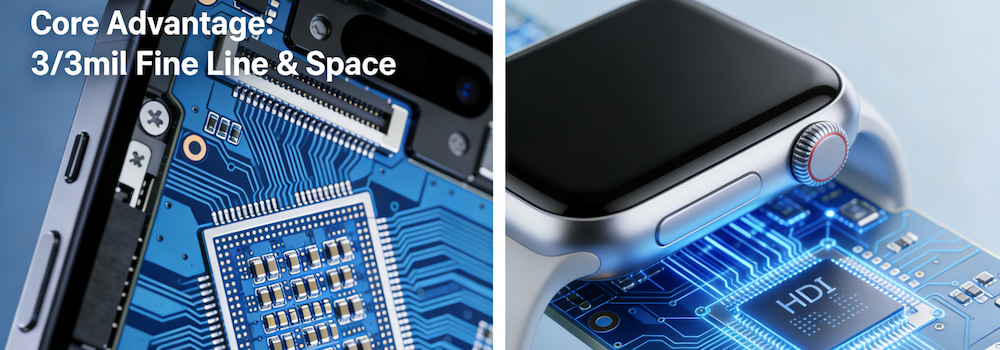
A. Space Magician: Higher Wiring Density
Technical Features: Supports extremely fine linewidths and pitches (typically 3/3 mil, advanced processes can reach 2/2 mil or even smaller), and widely utilizes microvias (diameter typically ≤0.15mm), blind vias, and buried vias.
Design Value: Allows for traces directly beneath the chip, perfectly supporting fine-pitch BGA, CSP, and QFN packages. This enables mounting components on both sides of the board, effectively doubling the component count.
B. Performance Booster: Superior Electrical Characteristics
Technical Features: Shorter electrical paths and fewer via fragments reduce signal loss.
Design Value: Reduced signal propagation delay and inductance/capacitance effects provide superior signal and power integrity. This is particularly crucial for consumer electronics like an Fan Motor Driver PCBA with Stepless Speed Control, where precise signal control and noise reduction are critical for user experience.
C. Reliability Guardian
Technical Features: Advanced stack-up structures and material selection (e.g., high-frequency/high-speed substrates).
Design Value: Better thermal management and mechanical stability, meeting the stringent reliability requirements of automotive electronics, aerospace, and medical fields (e.g., IPC-6012 Class 3 standard).
3. Key Considerations for Successful HDI Design
Early collaboration with HDI manufacturers is crucial for project success. Here are key points to communicate during the design phase:
- Define the Technology Level: How many layers of HDI does your design require? 1-layer (1+N+1), 2-layer (2+N+2), or any-layer? This directly determines cost and capability limits.
- Minimum Via/Pad Size: Clarify the limits for microvias to ensure manufacturability.
- Linewidth/Spacing Capability: Determine the minimum value (trace/space) that the manufacturer can reliably mass-produce.
- Layer Stack & Materials: Is it necessary to use low-loss (Low Dk/Df) materials to meet high-speed requirements?
- Design-for-Manufacturability (DFM): Reviewing the design with the manufacturer before production avoids costly rework.
4. Choosing a Professional HDI Manufacturer
When facing the complexities of HDI processes, choosing a partner with extensive experience is crucial. You need a manufacturer that offers comprehensive services.
Look for a provider capable of Custom PCB Fabrication. This ensures they have the mature process systems, advanced laser drilling equipment, and the ability to handle hybrid technologies required for complex projects.
 English
 日本語
日本語 한국의
한국의 中文
中文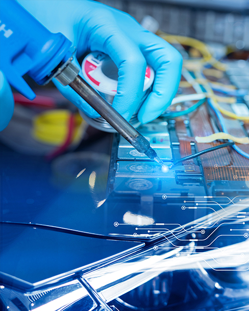


 IPv6 network supported