For mid-to-large enterprise hardware teams, ensuring field reliability and preventing batch defects in electronics manufacturing is critical. Evaluating quality goes beyond verifying electrical schematics; it requires rigorous inspection across automated production lines. Partnering with a reliable pcb layout company ensures that inspection requirements are integrated directly into the physical layout before manufacturing begins.
1. Automated Optical Inspection (AOI): SMT Surface Quality Shield
AOI systems use high-resolution cameras and machine vision algorithms to inspect surface-level assembly quality post-reflow.
Key Defects Detected : Component bridging (short circuits), tombstoning, missing parts, polarity reversal, and solder insufficient/excess.
Layout Requirement / Layout : Professional pcb layout services design clear clearance zones around components and place optical fiducials (Mark points) to enable automated alignment.
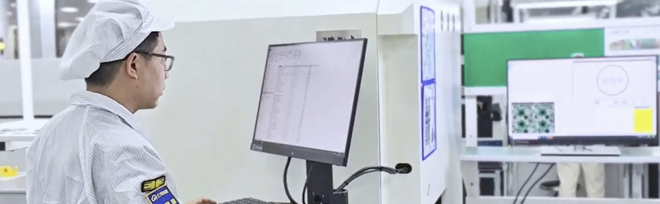
2. X-Ray Inspection: Unveiling Hidden Solder Joints (BGA / QFN)
Surface optical inspection cannot evaluate hidden pads under BGAs, QFNs, or bottom-terminated components (BTCs). X-Ray inspection passes through encapsulation to evaluate hidden solder structures.
Key Defects Detected : BGA solder voiding percentage, micro-bridging, head-in-pillow (HIP) defects, and solder ball cracking.
Layout Requirement / Layout : High-density HDI layouts built via professional pcb design services enforce proper thermal relief and pad geometries to prevent unequal heat distribution during reflow.
3. Functional Testing (FCT): Final Validation of Board Capabilities
While AOI and X-Ray check physical assembly integrity, Functional Testing (FCT) simulates real-world operating conditions by powering up the assembled board, injecting test signals, and measuring output responses via custom test fixtures (pogo-pin beds).
Key Objectives : Verifying voltage rail stability, firmware flashing, wireless communication strength, and sensor response times.
Layout Requirement : Engaging a team that provides turnkey pcb design ensures that dedicated test points (TP) are incorporated into the layout for test pin access without damaging fine-pitch signals.
Partner with Ruichun for Reliable PCBA Execution
Quality control begins at the layout stage. Ruichun integrates design, component sourcing, DFM auditing, and multi-tier inspection (AOI, X-Ray, FCT) into a seamless workflow. Visit www.ruichunpcba.com to get a quote and elevate your product's manufacturing reliability.
 English
 日本語
日本語 한국의
한국의 中文
中文





 IPv6 network supported